


#706 – Leading Edge Analog with Joren Vaes
Update: 2025-10-18
Description
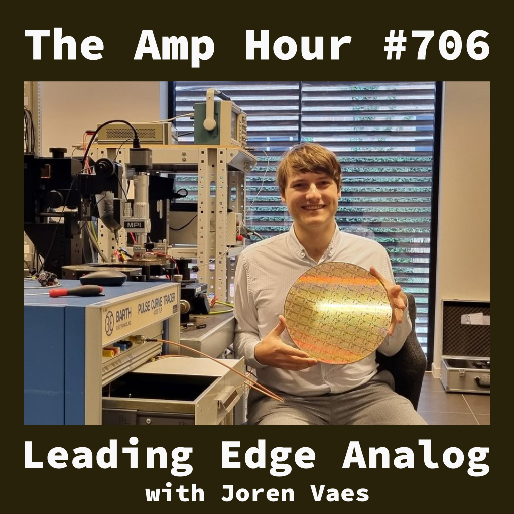
Welcome Joren Vaes, design engineer at SOFICS
- Simulation is critical when designing analog devices based on a PDK from the fab
- Parasitics are significant, especially with new nodes having upwards of 16 metal layers
- Chris complained about a class where the professor made them draw planar structures with graph paper with colored pencils
- Large fabs on leading edge nodes have 1800 page textbook of rules
- Because the constraints get tighter, that book gets longer for each node
- 2 nm mass production on finfet currently with TSMC
- 22 was the last classic cmos
- Finfet, looks like a devil
- ‘gate all around’ / nanosheet
- CFET (complementary field effect transistor) is next
- Joren really gets Maxwells Equations…as you have to at super high speeds
- SOFICS are making phy’s / IP blocks
- Amplifiers that are DC to 50 GHz
- Making a datasheet for the resulting IP block
- Joren got his PhD working on millimeter wave applications
- It’s all just physics
- Using coils to impedance match between layers
- Reflecting off of different materials at angles is Snells law (not lorentz equation) and that extends to different materials at different wavelengths
- Cables are very lossy at 100 GHz…dBs per cm
- Parasitics impact every part of the design process
- Wireline community – name for the high speed interfaces, including research in the space
- Most transistor threshhold voltages that Joren works with are … 750 mV!
- Voltage dependent drc rules
- Electromigration – holes in wires from electrons
- ESD is a big part of the business, and a large source of parasitics
- New product development for IP blocks
- Working with customers and Foundry at the 2 nm node
- Design companies need to be paying 100s of thousands to software providers
- After, it goes to spice and schedmatic
- Joren decides whether to jump in on layout
- LVS – layout vs schematic
- Parasitic extraction (spice netlist)
- PDKs define how you can do the layout stage
- Lower cost tools exist but more expensive tools have tooling that tells you when you’re violating DRC
- 3 main vendors
- Cadence
- Synopsis
- Siemens (Calibre)
- Foundries soemtimes only support one tool
- Doing test wafers allows testing of structures. They often get MPW at a discount from the fab (since they’re often testing new processes as well)
- How do they test with packaging options?
- ‘low speed’ can be die bonded or pcb mounted
- high speed does on wafer probing (with veeeery expensive probes)
- Check out Sofics.com for more info on the company. They also have a blog with a great name.
- Follow or connect with Joren on LinkedIn

Comments

In Channel

Download from Google Play

Download from App Store
 United States
00:00
00:00
1.0x

